Use "Initialize chain" instead.zeldaxpro wrote:I open up IMPACT, double click on the boundary scan and choose "add Xilinx Device".
Program Shuriken Video V3 Please Help!
Re: Program Shuriken Video V3 Please Help!
Asking for support by PM is anti-social. Ask in an open forum instead, so other people can benefit from the answers!

Re: Program Shuriken Video V3 Please Help!
Thank you Unseen and meneerbeer. I am making progress. I have shortened the JTAG wires significantly as I was doing some research and some people said do not have super long wires. I double clicked on Boundary Scan and Right clicked on Initialize Chain. I get an identity successful!!Use "Initialize chain" instead.
It then asks if I want to assign a configuration profile. I hit yes and choose the correct bit file
Then it asks if I want to attach an SPI or BPI. I hit yes and choose the .mcs
I hit ok right click on the chip and hit program
Program failed
At least that initialize chain shows that the chip is being recognized as far as I know. Anyone know what I am doing wrong or what the issue could be? Any help would be greatly appreciated! Thanks.PROGRESS_START - Starting Operation.
Identifying chain contents...'0': : Manufacturer's ID = Xilinx xc3s200a, Version : 0
INFO:iMPACT:1777 -
Reading C:/Xilinx/14.7/LabTools/LabTools/spartan3a/data/xc3s200a.bsd...
INFO:iMPACT:501 - '1': Added Device xc3s200a successfully.
----------------------------------------------------------------------
----------------------------------------------------------------------
done.
PROGRESS_END - End Operation.
Elapsed time = 1 sec.
// *** BATCH CMD : identifyMPM
// *** BATCH CMD : assignFile -p 1 -file "C:/Documents and Settings/AdminXP/Desktop/gcvideo-master/HDL/gcvideo_dvi/bin/gcvideo-dvi-shuriken-v3-2.1.bit"
'1': Loading file 'C:/Documents and Settings/AdminXP/Desktop/gcvideo-master/HDL/gcvideo_dvi/bin/gcvideo-dvi-shuriken-v3-2.1.bit' ...
done.
INFO:iMPACT:2257 - Startup Clock has been changed to 'JtagClk' in the bitstream stored in memory,
but the original bitstream file remains unchanged.
UserID read from the bitstream file = 0xFFFFFFFF.
INFO:iMPACT:501 - '1': Added Device xc3s200a successfully.
----------------------------------------------------------------------
----------------------------------------------------------------------
Selected part: M25P40
// *** BATCH CMD : attachflash -position 1 -spi "M25P40"
Unprotect sectors: FALSE
// *** BATCH CMD : assignfiletoattachedflash -position 1 -file "C:/Documents and Settings/AdminXP/Desktop/gcvideo-master/HDL/gcvideo_dvi/bin/gcvideo-dvi-shuriken-v3-2.1-spirom.mcs"
// *** BATCH CMD : attachflash -position 1 -spi "M25P40"
INFO:iMPACT - Current time: 8/11/2016 4:54:24 PM
// *** BATCH CMD : Program -p 1 -dataWidth 1
PROGRESS_START - Starting Operation.
Maximum TCK operating frequency for this device chain: 10000000.
Validating chain...
Boundary-scan chain validated successfully.
'1': Programming device...
LCK_cycle = NoWait.
LCK cycle: NoWait
done.
'1': Reading status register contents...
CRC error : 0
IDCODE not validated while writing FDRI : 0
DCM Locked : 0
status of GTS_CFG_B : 0
status of GWE : 0
status of GHIGH : 0
value of VSEL pin 0 : 0
value of VSEL pin 1 : 0
value of VSEL pin 2 : 0
value of MODE pin M0 : 0
value of MODE pin M1 : 0
value of MODE pin M2 : 0
value of CFG_RDY (INIT_B) : 0
DONEIN input from Done Pin : 0
SYNC word not found : 0
INFO:iMPACT:2219 - Status register values:
INFO:iMPACT - 0000 0000 0000 0000
INFO:iMPACT:579 - '1': Completed downloading bit file to device.
INFO:iMPACT:188 - '1': Programming completed successfully.
LCK_cycle = NoWait.
LCK cycle: NoWait
INFO:iMPACT - '1': Checking done pin....done.
'1': Programming terminated. DONE did not go high.
PROGRESS_END - End Operation.
Elapsed time = 0 sec.
zeldaxpro
Re: Program Shuriken Video V3 Please Help!
Two things:zeldaxpro wrote:At least that initialize chain shows that the chip is being recognized as far as I know. Anyone know what I am doing wrong or what the issue could be? Any help would be greatly appreciated! Thanks.
1) Impact only programs the chip that you selected - from the log you probably clicked on the FPGA, but you should click on the flash chip (small rectangle above the large square) instead and select "Program" there. For me, Impact sometimes reports failure even then - it shows in its log file that the flash chip was successfully programmed and verified, but its attempt to download the bitstream directly to the FPGA too failed with the same "DONE did not go high" problem. As long as the flash verification is successful this shouldn't matter though: If the DVI output works after power-cycling the Gamecube once, everything was programmed correctly.
2) It is possible that the download of the bitstream to the FPGA fails with the error you've encountered if the FPGA doesn't receive a stable clock signal (54MHz line) from the Gamecube.
Asking for support by PM is anti-social. Ask in an open forum instead, so other people can benefit from the answers!
Re: Program Shuriken Video V3 Please Help!
Thank you Unseen for your help and information I really appreciate it! So are you saying that it could of been programmed correctly already despite this error or? Do you think it could be like a hardware issue with the board or programmer? I will check the 54MHz line, as well as go through the process again by selecting the Flash instead of the FPGA.Two things:
1) Impact only programs the chip that you selected - from the log you probably clicked on the FPGA, but you should click on the flash chip (small rectangle above the large square) instead and select "Program" there. For me, Impact sometimes reports failure even then - it shows in its log file that the flash chip was successfully programmed and verified, but its attempt to download the bitstream directly to the FPGA too failed with the same "DONE did not go high" problem. As long as the flash verification is successful this shouldn't matter though: If the DVI output works after power-cycling the Gamecube once, everything was programmed correctly.
2) It is possible that the download of the bitstream to the FPGA fails with the error you've encountered if the FPGA doesn't receive a stable clock signal (54MHz line) from the Gamecube.
zeldaxpro
Re: Program Shuriken Video V3 Please Help!
Not according to the log you posted.zeldaxpro wrote:So are you saying that it could of been programmed correctly already despite this error or?
Probably hardware, but it could also be a programmer problem - the identification of the FPGA chip only needs to transfer a few bytes, the bitstream download sends much more.Do you think it could be like a hardware issue with the board or programmer?
Asking for support by PM is anti-social. Ask in an open forum instead, so other people can benefit from the answers!

Re: Program Shuriken Video V3 Please Help!
You can easily tell if it's programmed or not. I've done this 3 times (with shuriken video and original firmware) and worked as expected.zeldaxpro wrote:So are you saying that it could of been programmed correctly already ...
You only need GND and +3.3 (if have more wires don't remove them) after that get multi meter and check pin 1 if it reads 3.3v so it's programmed and working. Remove JP1 if connected.
If it doesn't work after all you can try my way. Buy CH341A programmer for about $2 and program *.bin file directly into flash memory. (It's not tested but should works I've made pretty much the same with pc's parallel port and homemade programmer.)
But first someone with the Xilinx software must create that file "promgen -spi -p bin -o spi_flash.bin -s 512 -u 0 toplevel_p2xh.bit".
Re: Program Shuriken Video V3 Please Help!
Hello TALANTO thank you for your help. So are you saying when I have my gamecube powered on and the shuriken video connected, I take my multimeter and read pin 1 and GND. If it reads 3.3v, it means it is programmed? Doesnt IMPACT have to say programmed successfully though? Because I have the error:TALANTO wrote:You can easily tell if it's programmed or not. I've done this 3 times (with shuriken video and original firmware) and worked as expected.zeldaxpro wrote:So are you saying that it could of been programmed correctly already ...
You only need GND and +3.3 (if have more wires don't remove them) after that get multi meter and check pin 1 if it reads 3.3v so it's programmed and working. Remove JP1 if connected.
If it doesn't work after all you can try my way. Buy CH341A programmer for about $2 and program *.bin file directly into flash memory. (It's not tested but should works I've made pretty much the same with pc's parallel port and homemade programmer.)
But first someone with the Xilinx software must create that file "promgen -spi -p bin -o spi_flash.bin -s 512 -u 0 toplevel_p2xh.bit".
LCK_cycle = NoWait.
LCK cycle: NoWait
INFO:iMPACT - '1': Checking done pin....done.
'1': Programming terminated. DONE did not go high.
PROGRESS_END - End Operation.
Elapsed time = 0 sec.
zeldaxpro
Re: Program Shuriken Video V3 Please Help!
Unseen said that it may be programmed so what I'm saying is just to check if it's working. It won't hurt trying but be careful with ESD (touch something earthed I almost killed my GameCube once).INFO:iMPACT:188 - '1': Programming completed successfully.
0. Disconnect JP1.
1. Desolder pin1 from GC. (optional but I recommend it)
2. Power the GC on.
3. Probe GND and pin1 on Shuriken Video board not GC side.
4. About 3.3v means working.
This is my theory:
If it's programmed and working properly has to pull high on pin1 [to tell the GC that component cable is connected].
If it's programmed wrongly it will fail the check sum and won't work [pin1 will stay dissconneccted].
If it's not programmed at all pin1 will stay dissconnected.
-
meneerbeer
- Posts: 212
- Joined: Wed Sep 03, 2014 9:13 am
Re: Program Shuriken Video V3 Please Help!
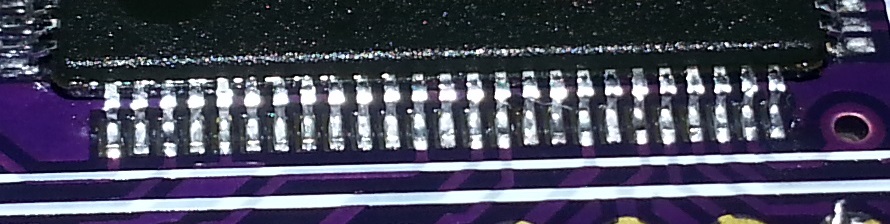
I still think there is a soldering problem somewhere. Perhaps try to gently tap all the pins on the FPGA to make sure all pins are connected.
Re: Program Shuriken Video V3 Please Help!
I make close up photos of FPGA pins and HDMI connector for shorts and bad solder joints and it works. Definitely use flux for the small pitch.
I use wide tip like this for soldering and it's really easy.
I use wide tip like this for soldering and it's really easy.
Re: Program Shuriken Video V3 Please Help!
meneerbeer wrote:I still think there is a soldering problem somewhere. Perhaps try to gently tap all the pins on the FPGA to make sure all pins are connected.
I don't know if this helps, but I uploaded pics of my board. I can't seem to find anything wrong by looking at it, but maybe I'm overlooking somethingTALANTO wrote:I make close up photos of FPGA pins and HDMI connector for shorts and bad solder joints and it works. Definitely use flux for the small pitch.
I use wide tip like this for soldering and it's really easy.
I am trying to eliminate one variable at a time. Would it be possible to program the board without the use of the Gamecube? I have a 3.3v regulator that I made I could probably use. What else would be needed in order to try it that way? Or any other possible things that I am doing wrong? Thank you.
zeldaxpro
Re: Program Shuriken Video V3 Please Help!
Did you measure pin 1?
Yes, you can put 3.3v and program without the gamecube.
I can't see shorts or anything wrong on your pictures. May try pictures on different angle where you can see that it's connected to pcb.
Also check 1.2v regulator if it's working.
Edit:
Is C8 tantalum and the right value? You may have power issue. It may not affect programming but later won't work.
Note: C7 should be 10uF and C8 should be 100nF so that the 3.3V supply rail raises before the 1.2V rail (next version going to have a proper reset IC).
- Attachments
-
- pins.jpg
- (93.71 KiB) Not downloaded yet
Re: Program Shuriken Video V3 Please Help!
Ok I will check to see if the 1.2v regulator is working. While powered on, I just take a multimeter to the input and then gnd pin to get a reading? C8 is not tantalum, but according to the build sheet part number from the BOM, it does not have to be (I also talked to happy_bunny on this). C7 is 10uF and C8 is 100nF (0.1uF).TALANTO wrote:Did you measure pin 1?
Yes, you can put 3.3v and program without the gamecube.
I can't see shorts or anything wrong on your pictures. May try pictures on different angle where you can see that it's connected to pcb.
Also check 1.2v regulator if it's working.
Edit:
Is C8 tantalum and the right value? You may have power issue. It may not affect programming but later won't work.Note: C7 should be 10uF and C8 should be 100nF so that the 3.3V supply rail raises before the 1.2V rail (next version going to have a proper reset IC).
When you say "measure pin 1", are you referring to pin 1 on the FPGA? (marked in yellow), or Pin 1 on the GC Pin (in red)? Thanks.
zeldaxpro
Re: Program Shuriken Video V3 Please Help!
To check 1.2v regulator power on and measure GND and output.
The yellow one is pin 26.
The red one and GND. If you have voltage (3.3v) it means that it's working. But you also may get 1.8v (or other voltage) from gamecube so I recommend removing pin1 from the GC before checking.When you say "measure pin 1", are you referring to pin 1 on the FPGA? (marked in yellow), or Pin 1 on the GC Pin (in red)? Thanks.
The yellow one is pin 26.
Re: Program Shuriken Video V3 Please Help!
Hey everyone I'm back with an update and still can't seem to get a program successful yet. To eliminate multiple variables I have the board hooked up directed to a 3.3v and GND power source. I have JP1 connected. I checked the 1.2V regulator and it is working (1.18-1.19 reading). I assign a configuration .bit, then the SPI .mcs for the M25P40. Still fails. However I am seeing that it's saying SPI not detected, so that may be the issue? Is there anyway to check to see if the M25P40 is working with a multimeter? Thanks.
zeldaxpro
-
meneerbeer
- Posts: 212
- Joined: Wed Sep 03, 2014 9:13 am
Re: Program Shuriken Video V3 Please Help!
Can you flash the .bit to the FPGA? You need to do that through JTAG and it will send the configuration bitstream to the FPGA. Once you power off the FPGA it "forgets" the configuration, which is why there is a flash chip to hold the configuration permanently.
Are you trying to program the board through JTAG currently? I think you should not connect the JP1 in that case, but I do not have the schematics.
Are you trying to program the board through JTAG currently? I think you should not connect the JP1 in that case, but I do not have the schematics.
Re: Program Shuriken Video V3 Please Help!
Thanks for the reply! Yes I'm currently trying to program the board via JTAG with the Xilinx Programmer and IMPACT. JP1 according to the schematic needs to be connected to directly program the flash device. I initialize chain, add the .bit and .mcs. When I click on the flash chip portion and hit program, it fails (pretty sure SPI not found?). When I click on the FPGA pic and hit program, it fails (DONE did not go high enough). It's not connected to the GC anymore it's directly 3.3v and GND. I can't seem to figure it out. Does anyone have any suggestions on what the issue is? I can post the log if that helps.meneerbeer wrote:Can you flash the .bit to the FPGA? You need to do that through JTAG and it will send the configuration bitstream to the FPGA. Once you power off the FPGA it "forgets" the configuration, which is why there is a flash chip to hold the configuration permanently.
Are you trying to program the board through JTAG currently? I think you should not connect the JP1 in that case, but I do not have the schematics.
On a side note I'm really thinking of trying to program this another way if possible. Has anyone had any luck with the method stated on happy_bunny's website, the CY7C68013A Mini Board (cypress FX2LP) method? Or any other methods at this point I just want to see this thing programmed and work.
zeldaxpro
-
meneerbeer
- Posts: 212
- Joined: Wed Sep 03, 2014 9:13 am
Re: Program Shuriken Video V3 Please Help!
If you want to program the flash through JTAG you do not need the jumper. You are now programming the flash through the FPGA instead of directly through the programmer.zeldaxpro wrote:Thanks for the reply! Yes I'm currently trying to program the board via JTAG with the Xilinx Programmer and IMPACT. JP1 according to the schematic needs to be connected to directly program the flash device. I initialize chain, add the .bit and .mcs. When I click on the flash chip portion and hit program, it fails (pretty sure SPI not found?). When I click on the FPGA pic and hit program, it fails (DONE did not go high enough). It's not connected to the GC anymore it's directly 3.3v and GND. I can't seem to figure it out. Does anyone have any suggestions on what the issue is? I can post the log if that helps.meneerbeer wrote:Can you flash the .bit to the FPGA? You need to do that through JTAG and it will send the configuration bitstream to the FPGA. Once you power off the FPGA it "forgets" the configuration, which is why there is a flash chip to hold the configuration permanently.
Are you trying to program the board through JTAG currently? I think you should not connect the JP1 in that case, but I do not have the schematics.
On a side note I'm really thinking of trying to program this another way if possible. Has anyone had any luck with the method stated on happy_bunny's website, the CY7C68013A Mini Board (cypress FX2LP) method? Or any other methods at this point I just want to see this thing programmed and work.
You only need to set the jumper if you program the flash directly with SPI. The jumper then makes sure the FPGA will not interfere/communicate with the flash.
Re: Program Shuriken Video V3 Please Help!
If that jumper controls the reset line on the FPGA, it indeed won't work at all if you have it connected. Flashing the SPI over JTAG requires downloading a special firmware to the FPGA, which will not be able to run if you hold it in reset.

Re: Program Shuriken Video V3 Please Help!
I am using the schematic posted by @happy_bunny to program a xc3s200a via my Parallel port. Also using fpga_flash.exe.
http://www.retro-system.com/shuriken%20video.htm
It is going very slow. So far over an hour and it says "programming at 25". Has anyone tried this method, and is it normal?
So after looking over alot of diagrams and posts, am I to understand that when deciding to flash via Parallel port, you solder connections directly to the flash? Not through the points a Programmer would connect to? I kept trying to match the traces of TD0, TD1, TMS, etc... to the equivilent points my Parallel port is connecting to. Also... the flash is programmed, not the FPGA itself?
Thanks for helping a newb understand better.
Is happy_bunny the creator of this?happy_bunny wrote:download/file.php?id=2000
http://www.retro-system.com/shuriken%20video.htm
It is going very slow. So far over an hour and it says "programming at 25". Has anyone tried this method, and is it normal?
So after looking over alot of diagrams and posts, am I to understand that when deciding to flash via Parallel port, you solder connections directly to the flash? Not through the points a Programmer would connect to? I kept trying to match the traces of TD0, TD1, TMS, etc... to the equivilent points my Parallel port is connecting to. Also... the flash is programmed, not the FPGA itself?
Thanks for helping a newb understand better.
Re: Program Shuriken Video V3 Please Help!
I just have a blank screen on HDMI (Shruiken v3). Gamecube still works over analog composite.
I programmed the flash via parallel last night. It appears to have completed. It took a few hours to complete. I did not close JP1.
I simply used the command:
fpga_flash.exe spi_flash.bin
I used the spi_flash.bin found among all the files in gcdv_update_0_5.zip
Do I want a different file to flash, for my xc3s200a?
Re: Program Shuriken Video V3 Please Help!
Some images to look at.
- Attachments
-
- 20161009_042906.jpg
- (3.07 MiB) Not downloaded yet
-
- 20161009_033603.jpg
- (2.89 MiB) Not downloaded yet
-
- 20161009_033842.jpg
- (2.59 MiB) Not downloaded yet
-
- 20161009_033546.jpg
- (3.23 MiB) Not downloaded yet
-
- 20161008_233810.jpg
- (2.96 MiB) Not downloaded yet
Re: Program Shuriken Video V3 Please Help!
We've discussed the slow programming with happy_bunny but he never fixed the old app. If you can recompile it just make all "sleep" "Sleep" (read the last pages viewtopic.php?f=3&t=2810&start=175 ). Of course you need another file for xc3s200a you can create it with Xilinx's software:
In your case probably won't work because of some checking. But you can damage you gamecube or TV with different bin file. It may send voltage on wrong pin.
If your fpga is soldered you should short JP1. Was the verifying successful without shorting?
You can probe the red one for voltage to see if it's working with the "wrong" fpga :
Code: Select all
promgen -spi -p bin -o spi_flash.bin -s 512 -u 0 toplevel_p2xh.bitIf your fpga is soldered you should short JP1. Was the verifying successful without shorting?
You can probe the red one for voltage to see if it's working with the "wrong" fpga :
Last edited by TALANTO on Mon Oct 10, 2016 9:56 am, edited 1 time in total.
Re: Program Shuriken Video V3 Please Help!
Super helpful! I'll get started and ask more questions as I try this. Thanks!
Re: Program Shuriken Video V3 Please Help!
Get the compiler from here 5.9.0 or newer. https://sourceforge.net/projects/orwell ... 0Releases/