GC HDD ADAPTER TUTORIAL
PARTS REQUIRED:
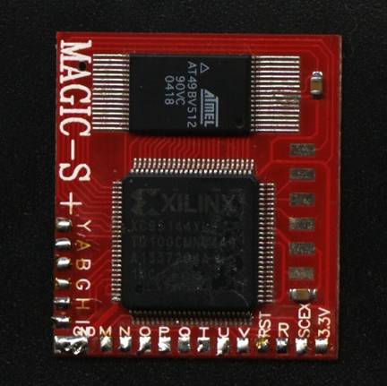
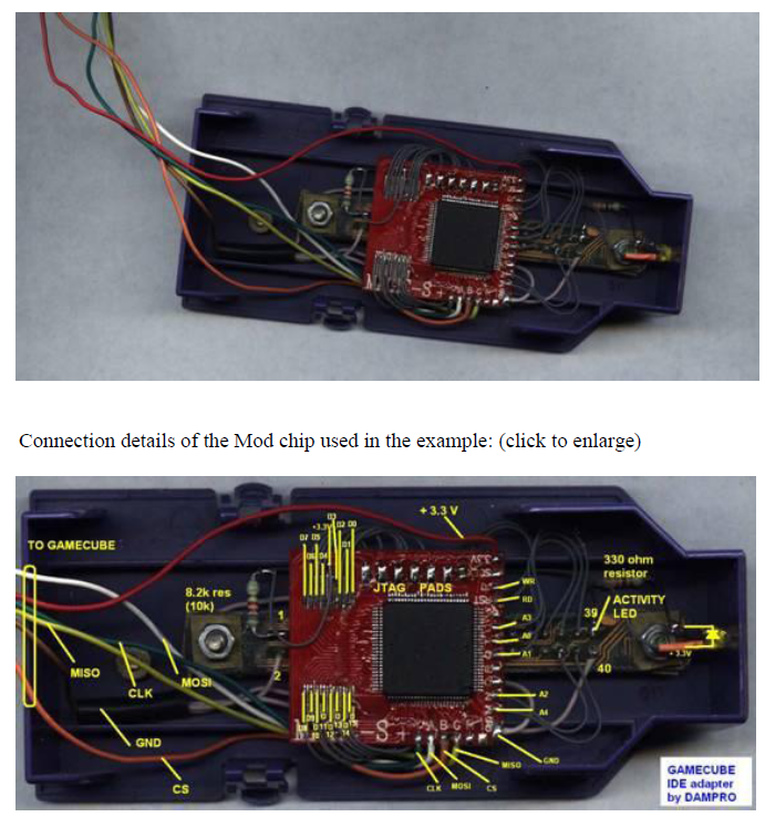
Part 1 – Old PS2 Mod chip (XILINX Based) … the best is RIPPER III clone, MAGIC-S or similar Mod chip
Preferably one with CPLD + parallel flash EEPROM...
(BLUECHIP and others that not use EEPROM can be used too, but this is more difficult as you’ll see later on)
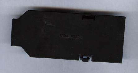
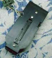
2 – Serial Port 1 cover, from GC (optional) J
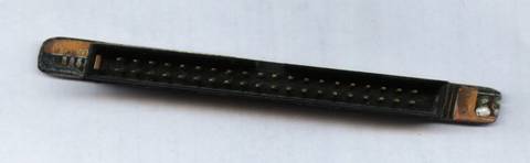
3 – Male IDE Connector (this one was taken from an old PC main board)
BUILDING THE ADAPTER:
Cut out a hole in the serial port cover to place the IDE connector, and make a small hole to put an activity LED:
|
|
|
|
|
|
|
|
|
|
|
|
|
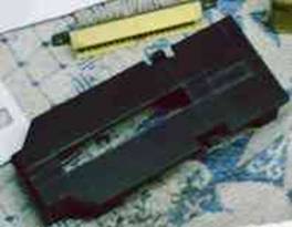
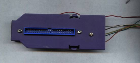
Secure the IDE connector to the cover, using screws and some nuts:
Building the
firmware & Re-programming the Mod chip to suit our needs: (hardest
part)
Uncompress the file "gcide.zip" ... inside you will find the firmware source!
Note: If you can obtain one of the following PS2 Mod chips: RIPPER III clone, MAGIC-S or BLUECHIP, you will only need to replace the file « gc_ide.ucf » with one of the files mentioned below, but make sure you use the correct one for your Mod chip!
gc_ide.ucf_BLUECHIP
gc_ide.ucf_MAGIC-S
gc_ide.ucf_RIPPER
If you’re using one of the above mod chips, rename the respective file to: gc_ide.ucf (overwrite the old one in the folder)
This file contains the pins assignments of the particular Mod chip. If you get a different mod chip from these, you need to check carefully the PCB and locate the needed pins, then edit the file.
Otherwise, you can skip the next step and go directly to programming the CPLD.
Configuring Pin
assignments:
(If using a Mod chip mentioned above, i.e. Ripper, Magic-S, Blue Chip, skip this step)
Below are the IDE signals used in the adapter.
You will need to assign one Mod chip PAD or CPLD pin to each IDE signal:
|
IDE Pin No. |
Drive Cable Signal name |
Signal Name in .ucf file |
|
1 |
RESET |
|
|
2 |
Ground |
|
|
3 |
D7 |
Ide_dat<7> |
|
4 |
D8 |
Ide_dat<8> |
|
5 |
D6 |
Ide_dat<6> |
|
6 |
D9 |
Ide_dat<9> |
|
7 |
D5 |
Ide_ dat <5> |
|
8 |
D10 |
Ide_ dat<10> |
|
9 |
D4 |
Ide_ dat <4> |
|
10 |
D11 |
Ide_ dat <11> |
|
11 |
D3 |
Ide_ dat <3> |
|
12 |
D12 |
Ide_adr<12> |
|
13 |
D2 |
Ide_ dat <2> |
|
14 |
D13 |
Ide_ dat <13> |
|
15 |
D1 |
Ide_ dat <1> |
|
16 |
D14 |
Ide_ dat <14> |
|
17
|
D0 |
Ide_ data <0> |
|
18 |
D15 |
Ide_ dat <15> |
|
19 |
Ground |
|
|
20 |
- |
|
|
21
|
- |
|
|
22 |
Ground |
|
|
23 |
WR |
Ide_wr |
|
24 |
Ground |
|
|
25 |
RD |
Ide_rd |
|
26 |
Ground |
|
|
27 |
- |
|
|
28 |
- |
|
|
29 |
Reserved |
|
|
30 |
Ground |
|
|
31 |
- |
|
|
32 |
- |
|
|
33 |
A1 |
Ide_adr<1> |
|
34 |
- |
|
|
35 |
A0 |
Ide_adr<0> |
|
36 |
A2 |
Ide_adr<2> |
|
37 |
A3 |
Ide_adr<3> |
|
38 |
A4 |
Ide_adr<4> |
|
39 |
DASP |
|
|
40 |
Ground |
|
(Table 1)
And these are the EXI signals:
|
exi_clk |
|
exi_cs |
|
exi_out |
|
exi_in |
If you need to edit the .ucf file, the format of this is simple, for example:
NET "exi_clk" LOC = "P97" ; --> signal "exi_clk" located to pin 97 of the CPLD
.
.
NET "ide_adr<1>" LOC = "P13" ; --> signal "ide_adr<1>" to pin 13 of the CPLD
And so on ... you need to locate at least 27 pins that have traces and if possible PADS to solder easily.
That is why the better Mod chips are the ones that use a parallel EEPROM, since they have plenty of pins easy to trace and PADS attached on to solder to!
Other Mod chips can also be used, like the BLUECHIP, but these do not use EEPROM and only 23 pins have traces, therefore you’d need to solder direct to the CPLD pins.
Building the
firmware:
Now, we’ll need to build the project with XILINX ISE...
Go to the Xilinx web site and register so you can download their free ISE Web Pack software which we’ll use to program the CPLD:
http://www.xilinx.com/products/design_resources/design_tool/index.htm
Install it, and open project file « exi2ide.ise » then right-click the Implement Design process in the Processes tab, and select « Rerun All ».
Wait until the implementation completes. (Ignoring the warnings)
Building the JTAG
Cable and Programming the CPLD:
The above process will generate a programming file named « gc_ide.jed » that you will need to program onto the CPLD.
To do that, only you need a simple JTAG cable, like the one below (which can be easily made at home):
http://warmcat.com/milksop/cheaptag.html
Now we’ll use a tool called iMPACT to program the CPLD.
This tool is located in the Processes tab.
Click Generate Programing file – Configure device (iMPACT)....
Complete details of this can be found in the attached documentation, or see the link below:
http://www.dspassme.com/docs/html/pm_04_programming_cpld.html
Soldering it all
together:
Once the chip is reprogrammed, we’ll need to wire it to the IDE connector:
(Some good soldering skills are needed)
At IDE connector level:

(Refer to table 1) When building the adapter, all grounds (GNDs) go directly to GND of the Gamecube.
Connect Pin 1 (RESET) to a PULL UP (10K) to 3.3v and Pin 39 (DASP) is output to LED indicator of drive activity.
After this, the adapter is complete and ready to be hooked up to our Gamecube!
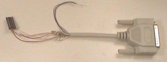
Set up EXI signals to the Gamecube... and we’re done! (Use memory card slot B)
|
Pin |
Signal name |
Used Color |
|
|
1 |
EXTIN |
|
Connected to Pin 12, EXTOUT |
|
2 |
GND |
|
Ground |
|
3 |
|
|
|
|
4 |
3.3V |
Red |
+3.3V supply |
|
5 |
DO |
White |
MOSI - Master OUT, Slave IN |
|
6 |
|
|
|
|
7 |
DI |
Yellow |
MISO - Master IN, Slave OUT |
|
8 |
3.3V |
Red |
+3.3V supply |
|
9 |
CS |
Blue |
Device select |
|
10 |
GND |
|
Ground |
|
11 |
CLK |
Green |
Clock |
|
12 |
EXTOUT |
|
To Pin 1, EXTIN |
Notes:
Pins 1 (EXTIN) to 12 (EXTOUT)
Pins 2, 10 (GND) connected to ground
Pins 4, 8 (+3.3V) supply
Credits:
Many thanks to all contributors that helped me in collaborating this project in one way or another:
- tmbinc (debugmo.de) (his great work is the base of the actual GC and Wii scene, this project inclusive)
- xt5 (ingenieria-inversa.cl)
- nuke (USB Gecko)
- emu_kidid (for SD-Boot and other great GC homebrew)
- and the countless others who have helped along the way :)