all the methods described across the various sites show various processes from simple to complicated..
for a beginner, it can be an overwhelming amount of data to determine which method is the best or best suited..
especially when everyone claims their method is the best because they have tried all the other methods...
and to add to the confusion is the various types of PCB software, transfer methods, transfer materials, etching solutions, pcb board material type, copper weight, where to buy materials, and other crap people want to discuss..
in the end, the very basic and simple idea is to cover the copper you want to keep, all other exposed copper will be etched..
where to begin describing the differences of these methods is even more complicated than describing the methods themselves due to the fact there is so much to consider to achieve the board you want...
even if you want to experiment just to get an idea of how a process works is not as simple because it requires a decision of a method to utilize and possible extra investment based on that decision..
one thing i can guarantee, you will spend money and spend more money as your technique improves or in attempts to improve...
i believe the most important consideration for a method of choice is based on the types of components used on the board as well as the size constraints of the board...
to say this another way, the bigger the components and the more board space you have, the more forgiving the method to allow wider circuit traces...
the smaller the components and the smaller the design, the tighter the tolerance for circuit traces and more accuracy required...
transfer methods:
just to get a design onto a board can range from simple to complicated..
as stated, the most important consideration for the method of choice depends mainly on accuracy requirements..
sharpie marker
IMO, the most simplest cost effective method is to use a sharpie marker
the marker is used to free hand draw a circuit, or even just draw a few shapes for experimenting..
this is best for beginners or when in need of a quick and dirty circuit board...
the advantage, no need to learn PCB software...wipes clean with acetone..
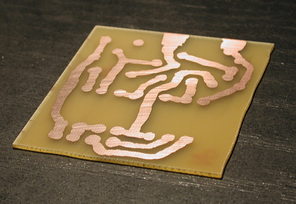
the disadvantage, its a free hand drawing and will only look as good as your steady hand allows...also, traces are limited to the width of the marker
heat transfer method
heat transfer is probably the most used, most discussed method method on the web
why? it works and its cheap..(depending)
also, cheap only if you already own a laser printer as all heat transfer methods require a laser printer...
why? the ink used in laser printers can be reheated with any clothing iron that stick the ink onto the copper...
there are many heat transfer paper materials that can be used to apply the circuit to the board..
but before transferring the design, the design must be created using PCB software to print onto a paper material of choice..
the cheapest is a pack of 300 sheets of laser printer photo paper http://www.staples.com/Staples-Color-La ... uct_633215
a more expensive option is to use Press-n-peel Blue http://www.techniks.com/
also expensive is toner transfer paper http://www.transfermagic.com/ (i think this is the only method that allows ink jet printers but results vary)
the good thing about the photo paper is you get 280 more sheets of paper at half the cost of 20 press-n-peel
i never used press-n-peel even tho people claim to have very good results
with practice to develop proper technique of iron temp, applied pressure and heating time, very good results can be achieved using photo paper..
photo paper advantages and disadvantages...
main advantage is its cheap and wipes clean with acetone..
good results can be had with proper technique..
disadvantages...after iron on, the board/paper must be soaked in water to allow the paper to come off..
light rubbing of the paper is also required during the soak process which can accidentally pull ink traces off board..
if this happens, wipe the board clean with acetone and try again...
press-n-peel advantages and disadvantages...
main advantage is (supposedly) easier iron method for beginners and or better accuracy for experienced users
the main disadvantage is the cost...
( i dont think the cost is worth it)
after etching, the press and peel must be scrubbed off with steel wool (unlike photo paper with an easy wipe of acetone)
toner transfer paper i do not know about but it allows use of ink jet printers and does not always have consistent results..
any heat transfer method will have one main disadvantage...
the ink must be heated in order for it to stick...this means it has to melt...
melting means a small loss of pattern shape, this can be a very important factor if board design requires very close traces or close component placement
why? traces and or component pad can melt together
only practice of technique will help this, but sometimes technique will never make a difference if trying to design a board for smaller pitch components...(for example: xilinx)
second disadvantage to heat transfer method with photo paper (and as ive read about peel-n-press)... a sharpie marker may be required for touch ups on traces and pads which then adds all the mentioned disadvantages of using a free hand sharpie to draw the touch ups...
third disadvantage to the heat transfer method is the paper is use once...
this means results will vary if making several of the same type of board..and increased chance of improper transfer with the more boards produced...
fourth disadvantage is making double sided PCBs can be difficult to achieve ...especially when the potential exists to underheat the toner resulting in the toner not to stick to the copper or overheat the toner resulting in the toner to smear and run together...
UV transfer method
i never thought the day would come where i would find myself using a UV transfer method to make PCB's...especially when i have been so successful in the past using photo paper and an iron...
i have mentioned several times during describing the heat transfer method about technique..
technique plays a large role in proper heat transfer process...and can also be the most time consuming part of making a PCB due to improper technique, inadequate transfer, touch ups, or clean up and redo
with UV transfer, about the only technique required is opening a beer and finishing it within about 10 minutes during waiting time of UV exposure...
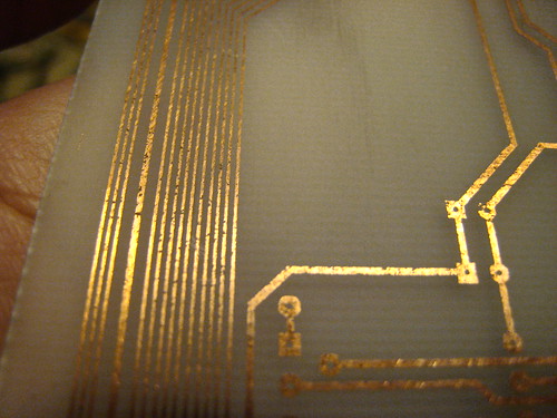
of course, UV transfer requires a UV source and UV sensitive PCBs, i believe this to be the most simple PCB making process to achieve a very high accuracy with little effort and no prior experience..
UV transfer ( as with heat transfer ) requires a PCB software to be utilized to print the design
however, rather than using an iron to heat ink in attempts to transfer the ink from paper to copper, the circuit design is printed to a transparency sheet (remember grade school with overhead projector??) which is placed on top of the PCB and exposed to a UV light source with the printed traces blocking UV exposure..
the blocked traces (or pattern) will act as an etch resist in the same manor as physical ink on the copper...
after UV exposure, the board is dipped in a special solution to remove the UV sensitive film which has been exposed to UV light and then the board is ready for etching...
there is really not much more to describe about the UV transfer method other than to build or buy a UV light box...
i built one using a simple tupperware box and the LED circuit described in this instructable http://www.instructables.com/id/UV-LED-Exposure-Box/
exposure time is about 8-10 minutes with the PCB about ~75mm or ~3" from the light source
overexposure means you lose the traces, under exposure means you dont have traces...
the LED circuit design described in the instructable only requires 8-10 minutes
my simple tupperware UV exposure box...

advantages:
transparency sheets are sold for both laser and ink jet printers...
transparency sheets are about 40$ for 50 sheets, but are the sheets are also reusable...
board production (or reproduction) consistency has an extremely high rate of guarantee...
beginner to advanced user can easily produce accurate PCBs...
developer solution is usually included with the PCB ( on ebay purchases )
developer solution mixture is reusable for many boards
double sided PCB's are much easier to create/recreate..since its easier to align land marks using transparency sheets
photosensitive PCBs are just a bit more expensive but seems easier to work (definitely worth minimal extra cost for beginners or lazy developers)
cheap UV LED's can be found on cheap on ebay.... about ~5$ for 100 LED's
disadvantages:
transparency sheets are about 40$....but as previously stated sheets are reusable
photosensitive PCB's can cost more (i have found the cheap Chinese boards from ebay to be sufficient compared to some more expensive boards)
ebay boards only come in 1.6mm board thickness...thinner boards cannot currently be found on ebay and must be purchased thru other vendors
cost comparison of PCB's:
120mm x 180mm non presensitized PCB = about 3.25$
100mm x 150mm presensitized UV PCB = about 4$
slightly more expensive but IMO worth the extra minimal cost...
final overview
a sharpie marker is great for quick drawing to make a PCB really fast that is not too complicated and can also be good for guinea pig testing of etching solution to determine etching times
heat transfer can be a cheap and quick start up method. This is widely accepted as the normal method for home PCB production..
once proper technique has been achieved, most any PCB design can be created
UV transfer is phenomenal for creating consistent and accurate PCBs with little to no effort involved..
i have used heat transfer for years with great success and not to mention multiple redo's in order to achieve success...
had i known and tried UV transfer sooner, it would have made my life easier...
i dont know if i will ever use heat transfer method again now that i have been "exposed" to UV transfer....
my recommendations, first use heat transfer with photo paper and go to home depot and buy a gallon of acetone...
once you get lazy or feel the need for better accuracy then move on and use UV transfer
or better yet, if you committed to making PCB's just save yourself the trouble and start with a UV setup....
or maybe use the heat transfer method to start off with to gain more appreciation for UV transfer...


